Universal Notch and Bandpass Filter
Randy Hargenrader, WJ4P Summerville, SC USA email:
The one feature I seem to use very often when operating is the audio notch filter. It is an interesting tool. For example, besides the obvious notching of offending signals in the pass-band, I find that for weak signals, sometimes putting the notch "beside" the signal helps you hear the target signal better. I think that what happens is the notch removes some of the noise near the audio frequency of the signal, improving the perceived "signal to noise ratio". I originally designed this filter circuit for my Elecraft K2 transceiver but I quickly realized that it was applicable to other rigs as well. My OHR-400 will be sporting one of these very shortly!
The design uses a switched capacitor filter IC, the LTC1059, which is Linear Technologies’ version of the venerable Texas Instruments MF5C. This IC uses a clock signal at 50 or 100 times the frequency of interest to determine the resonant frequency of the notch or bandpass. This IC has various modes of operation and the mode I employed allowed both the notch and bandpass functions from the same circuit. Other modes of operation can focus on other functions such as high-pass and low-pass filtering.
The slope of the notch function for this design is about 65Hz wide at the -3dB points and gets narrower as it gets deeper. I couldn’t measure the bottom of the notch with my setup using Spectrogram or with the meters I have in the shack. The signals that are notched do receive a great deal of attenuation, in the order of 30 dB or more. The IC specs predict -50dB of attenuation in this mode.
This filter also has a bandpass function, which has been fun to experiment with. It has been quite useful even with the narrow IF filter settings available in the K2. It gives about 3dB gain to the signal you want, but it does attenuate the other frequency signals depending how far away they are from the center frequency. The slope of the bandpass filter mode is about 115Hz wide at -3dB, with a total attenuation of -15dB or so for the rest of the audio band.
This circuit adds about 12 mA to the current consumption of the radio.
The Circuit
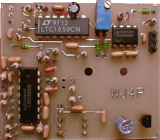
The circuit schematic is shown at the bottom of the next page. The small PC board that I made is shown in the following photo.
The K2 required a balanced input and output arrangement. This was accomplished by using a single op-amp for the input and a pair of op-amps for the output. I used LM3900 op-amps because I have a bunch of them around and I am familiar with them. Another op-amp can be used but will require a slightly different circuit to allow for the usual input biasing. The LM3900 is a Norton input type op-amp and can be biased with a single resistor.
For radios that use unbalanced audio circuitry, the op-amp circuits can be modified appropriately. The op-amp circuitry was designed to provide unity gain through the filter. If you would like to have this circuit provide some gain to the audio section, I recommend that you match the value of the input resistors to either the input or output op-amp circuitry. Do not change the feedback resistors as they are set to work with the biasing resistor values. To get more gain from this circuit design, change the input resistors to a lower value. (Remember op-amp theory, the gain is determined by the ratio of the input and feedback resistors.)
There is no on-off switch so it is always "active". You take the filter "off line" by putting it in the notch mode and setting the frequency control at one limit or the other a la TenTec style.
I used a TLC555 (CMOS 555 timer) as the clock generator. This part is good to about 2 MHz in astable mode. VR1 controls the frequency by presenting voltage to the control pin. This arrangement keeps the R/C circuit nice and tidy right by the IC, reducing radiation from that circuitry. Since I used the 100X configuration for the clock input, it requires that the clock frequencies range from about 30,000Hz to about 300,000Hz to give a filter resonance of 300Hz to 3000Hz.
Even though this is an audio circuit, it uses a fairly high frequency clock signal so it is important that when you build the circuit you keep the LTC1059 connections as short as possible. The clock signal from the 555 timer should also be very direct and short.
Adjustment
Adjusting the filter clock circuit to the correct frequency range is accomplished using an oscilloscope or a frequency counter connected to pin 8 of the LTC1059. As stated before, the frequency control pot uses a voltage to control the astable frequency of the 555 timer. This form of control on the TLC555 timer allows a range of 10:1 from lowest to highest frequency. I selected the range of 300Hz to 3000Hz for my notch and passband. To adjust the clock frequency, position the frequency control pot to the low frequency limit and set R2 for 30KHz. Then turn the frequency control pot to the high frequency limit and check that it is operating at about 300KHz.
If you elect to use the oscilloscope method, follow these steps. The waveform from the 555 timer is asymmetrical, with low going pulses of about 5µs in duration. The period of this waveform is the total time from similar points on the waveform. Turn the frequency control pot to the low frequency limit and adjust R2 on the filter board to set the waveform for a period of 33.3 µs. This sets the lower frequency limit to 300Hz. The clock at this frequency is 30KHz for the 100X clock input to the LTC1059. Next, turn the frequency control pot to the high end and verify that the period of the signal is about 3.33 µs
Installation
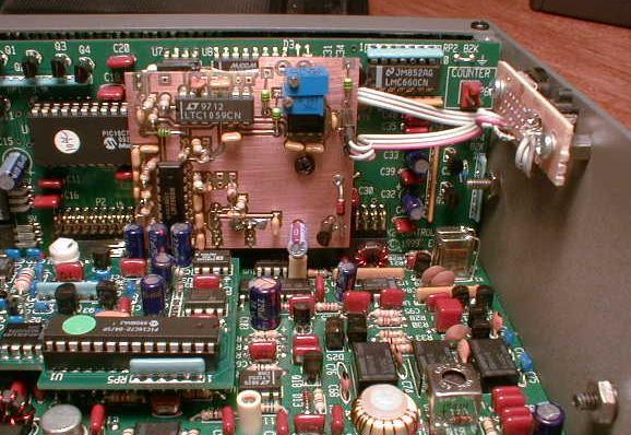
I elected to install this board inside my K2. The operating controls needed to be located where I could easily get to them when operating. As you can see from one of the pictures, the frequency potentiometer and the slide switch, both salvaged from a defunct cassette player, were installed on a piece of perf-board. That, in turn was mounted to the inside top edge of the side panel. That would allow me to notch out a place on the top panel for each control. I chose the left side since I am right handed and usually use my left hand to operate the radio. I believe I measured the notch locations about 6 times before actually taking a deep breath and using the nibbler tool!
The internally mounted board fits right on the Control Board and uses the audio filter option headers for insertion into the audio path. The board is held in place by using the audio filter option stand-off located between the two electrolytic capacitors (see photo). For more information and photos on installing the filter in a K2, visit the Elecraft web site at www.elecraft.com and click on the "Tech Notes" link.
Adaptations
This circuit can be added to just about any radio. For an unbalanced audio path, just use conventional op-amp unbalanced circuit connections. You will only need one of the output op-amps to output unbalanced audio. On the input, connect the audio signal to the inverting input and leave the other (non-inverting input) unconnected. There is no need to ground the unused input.
Although the entire circuit will run on 12 volts DC, I used an eight-volt regulator to stay compatible with the K2’s circuitry. The DC voltage from the output op-amps is used to bias FET audio switches in a further stage. It is important that you be aware that there are no capacitors coupling the outputs of the op-amps. Your radio might require some DC isolation to keep from unintentionally biasing the next stage.
Edited by W1HUE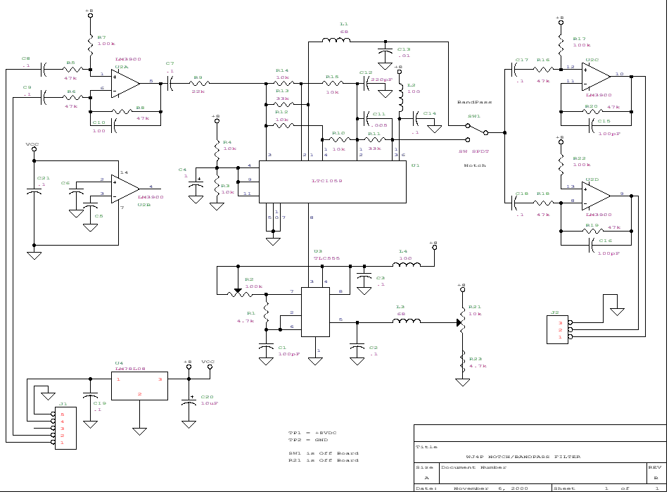
Click here for pdf version of schematic. Adobe Reader Required.